Google Cloud Releases New TPU Chip Lineup in Bid to Speed Up AI - Bloomberg
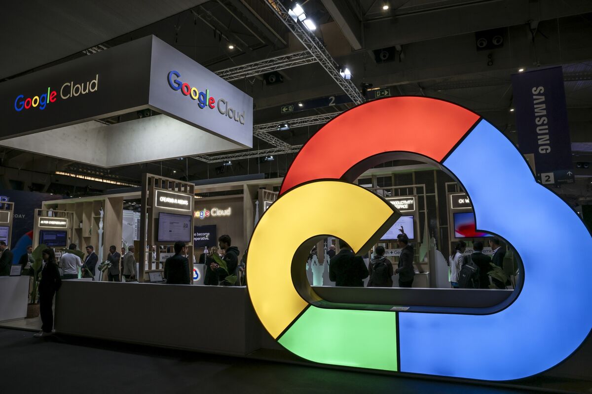
```json { "title": "Google Unveils 8th-Gen TPU Chips to Power the AI Agentic Era", "metaDescription": "Google Cloud launched TPU 8t and TPU 8i at Cloud Next 2026, splitting its flagship chip into two purpose-built architectures for training and inference.", "content": "<h2>Google Cloud Launches TPU 8t and TPU 8i at Cloud Next 2026</h2><p>Google Cloud made its most architecturally significant chip announcement in the history of its Tensor Processing Unit program on April 22, 2026, unveiling two eighth-generation TPUs at its annual Cloud Next event in Las Vegas. For the first time, the company split its flagship TPU into two entirely distinct, purpose-built chips: the <strong>TPU 8t</strong>, optimized for large-scale model training, and the <strong>TPU 8i</strong>, optimized for inference and reinforcement learning. The move marks a deliberate departure from the one-size-fits-all chip design that characterized all previous TPU generations.</p><p>The announcements were made alongside a $750 million partner fund and a sweeping capital expenditure commitment from CEO Sundar Pichai, signaling that Google is accelerating its AI infrastructure buildout at a pace few companies can match.</p><h2>TPU 8t: Massive Scale for Model Training</h2><p>The TPU 8t is built for the computationally intensive work of training frontier AI models. A single TPU 8t superpod packs 9,600 chips, delivering 121 exaflops of compute and two petabytes of shared high-bandwidth memory (HBM) connected through high-speed inter-chip interconnects. For context, the previous seventh-generation chip, Ironwood, offered 9,216 chips per pod with 42.5 exaflops — the new chip represents nearly a three-times improvement in raw compute performance.</p><p>Google claims the TPU 8t delivers up to 2.8x better performance per dollar compared to Ironwood for large-scale training workloads. According to Google, the performance gains are substantial enough to cut development cycles for frontier AI models from months to weeks.</p><p>The scale of deployment enabled by the TPU 8t is notable. Using its Virgo Network fabric, Google says it can connect 134,000 TPUs in a single fabric within one data center and link more than one million TPUs across multiple data center sites into a single training cluster. Both chips run on Google's in-house Axion ARM-based CPUs and use fourth-generation liquid cooling technology. The TPU 8t was designed with chip partner Broadcom, which handled complex silicon implementation, high-speed SerDes interconnects, and advanced packaging.</p><h2>TPU 8i: Breaking the Memory Wall for AI Inference</h2><p>The TPU 8i is engineered specifically for the demands of AI inference — the process of running a trained model to generate outputs — and for what Google calls the "Agentic Era," in which AI systems must reason, plan, and execute complex multi-step tasks simultaneously and at scale.</p><p>The chip triples on-chip SRAM to 384 MB and increases HBM to 288 GB compared to its predecessor, enabling massive key-value (KV) caches to be hosted entirely on silicon. This is designed to support low-latency agentic workflows where speed of response and context retention matter most. The TPU 8i also doubles inter-chip interconnect (ICI) bandwidth to 19.2 Tb/s and reduces the ICI network diameter by more than 50%. A new dedicated Collectives Acceleration Engine (CAE) reduces on-chip latency by up to 5x.</p><p>Google claims the TPU 8i delivers 80% better performance per dollar for inference compared to the Ironwood generation.</p><p>The chips are integrated into Google's AI Hypercomputer platform, paired with the Virgo data center fabric and Google Cloud Managed Lustre storage, which now delivers 10 TB/s of storage bandwidth — a tenfold improvement over the prior year.</p><h2>The Strategic Shift: Specialization Over Generality</h2><p>The decision to bifurcate the TPU family is the central strategic signal of this announcement. Previous TPU generations were designed to handle both training and inference on a single chip architecture. The new dual-chip approach reflects the changing demands of AI workloads, particularly as agentic AI systems — which must perform continuous inference at low latency while also supporting ongoing model refinement — become the dominant use case for enterprise customers.</p><p>Google Cloud CEO Thomas Kurian declared at Cloud Next 2026 that the experimental phase of artificial intelligence is over, framing the new chip generation as infrastructure for a new operational reality rather than a research tool.</p><p>The announcement also came with a broader financial commitment. Sundar Pichai announced that Google plans to invest between $175 billion and $185 billion in capital expenditure in 2026 to build AI infrastructure — a figure that dwarfs the company's $31 billion in capital expenditure in 2022. Google Cloud, which holds roughly 11% of the cloud infrastructure market, grew at 48% in the fourth quarter of 2025, underscoring the commercial momentum driving these infrastructure bets.</p><p>Pichai also noted that Google Cloud's first-party models now process more than 16 billion tokens per minute via direct API use by customers, up from 10 billion the prior quarter — a metric that illustrates the raw demand the new chips are being built to serve.</p><p>Additionally, Google announced a $750 million fund directed at its 120,000-member partner ecosystem, which includes global consulting firms, systems integrators, software partners, and channel partners. The ecosystem includes more than 330,000 experts trained on implementing Google AI for customers.</p><h2>Real-World Deployments and Industry Partnerships</h2><p>Google highlighted several existing deployments of its TPU infrastructure that illustrate the commercial reach of its chip program. Citadel Securities has built quantitative research software that draws on Google's TPUs. All 17 U.S. Energy Department national laboratories use AI co-scientist software built on the chips. Anthropic, the AI safety company, has committed to using multiple gigawatts' worth of Google TPUs.</p><p>On the competitive front, Google also announced a collaboration with Nvidia to engineer computer networking — specifically the software-based networking technology called Falcon — that allows Nvidia-based systems to perform more efficiently in Google's cloud. This move positions Google as a platform that can support both its own custom silicon and third-party GPU infrastructure, rather than treating the two as mutually exclusive.</p><h2>Expert Reactions</h2><p>Amin Vahdat, Google's Senior Vice President and Chief Technologist for AI and Infrastructure, explained the rationale for splitting the chip into two architectures: <em>"With the rise of AI agents, we determined the community would benefit from chips individually specialized to the needs of training and serving."</em></p><p>On the TPU 8i's memory capabilities specifically, Vahdat said: <em>"We've finally broken the memory wall that slows long context decoding."</em></p><p>Sundar Pichai framed the announcements in the context of Google's long-term infrastructure strategy: <em>"As we move into the agentic era, we are taking this to the next level. We are making big investments now and for the future."</em></p><p>On the scale of model usage on Google's infrastructure, Pichai stated: <em>"Our first-party models now process more than 16 billion tokens per minute via direct API use by our customers, up from 10 billion last quarter."</em></p><p>Scott Alfieri, Accenture Google Business Group Lead at Accenture, commented on the $750 million partner fund: <em>"Google Cloud's investment strengthens how we solve complex technical challenges and build enterprise-ready solutions together, accelerating the adoption of Gemini Enterprise, modernizing digital cores, and helping clients realize tangible outcomes from agentic AI faster."</em></p><h2>What Comes Next</h2><p>The TPU 8t and TPU 8i are now part of Google's AI Hypercomputer offering, available to Google Cloud customers. The chips represent the eighth generation of a program that has iterated continuously since Google first deployed TPUs internally to power products like Search, Maps, and Photos — all of which serve over one billion users.</p><p>The broader competitive landscape remains active. AWS has its own custom silicon program with Trainium3, and Nvidia continues to dominate the GPU market for AI workloads. Google's dual-chip strategy and its willingness to also deepen collaboration with Nvidia on networking suggest the company is pursuing a platform approach — optimizing its own silicon for specific workloads while ensuring its cloud remains compatible with the broader AI infrastructure ecosystem.</p><p>With nearly 75% of all new code at Google now AI-generated and approved by engineers — up from 50% the prior fall, according to Pichai — the company is also one of the most intensive internal consumers of the infrastructure it is selling. That self-referential scale may be one of the clearest signals of where enterprise AI infrastructure is heading.</p><p>For more tech news, visit our <a href=\"/news\">news section</a>.</p><h2>Why This Matters for Your Productivity</h2><p>Faster, more efficient AI infrastructure directly shapes the tools that knowledge workers, health professionals, and productivity-focused individuals use every day — from AI assistants that can hold longer context and respond more quickly, to enterprise platforms that surface insights with less latency and more accuracy. As the underlying chips that power these tools become more specialized and capable, the software built on top of them will follow. Staying informed about these shifts helps you make smarter decisions about the platforms and tools you rely on. <a href=\"/#waitlist\">Join the Moccet waitlist to stay ahead of the curve.</a></p>", "excerpt": "Google Cloud unveiled two eighth-generation TPU chips at Cloud Next 2026 in Las Vegas — the TPU 8t for large-scale AI training and the TPU 8i for inference — marking the first time the company has split its flagship chip into two purpose-built architectures. The announcements came alongside a $175–$185 billion capital expenditure commitment from CEO Sundar Pichai and a $750 million partner fund. The move signals a strategic shift toward specialized silicon designed for the demands of agentic AI systems.", "keywords": ["Google TPU 8t", "Google TPU 8i", "Google Cloud Next 2026", "AI chip training inference", "agentic AI infrastructure"], "slug": "google-8th-gen-tpu-chips-agentic-era-cloud-next-2026" } ```